Home
/ Mosfet Working Gif - Mosfet Und Metalloxid Halbleiter Tutorial : Animated diagram showing the operation of a tuned circuit (lc circuit).
Mosfet Working Gif - Mosfet Und Metalloxid Halbleiter Tutorial : Animated diagram showing the operation of a tuned circuit (lc circuit).
Mosfet Working Gif - Mosfet Und Metalloxid Halbleiter Tutorial : Animated diagram showing the operation of a tuned circuit (lc circuit).. The invention of transistors revolutionized human civilization like no other technology. Some gif animations or java applets could have enhanced learning experience. The best gifs for mosfet. I've been thinking about using the dn2540 mosfet in my next amp as a split load phase inverter. Animated diagram showing the operation of a tuned circuit (lc circuit).
Mosfet working animation | mosfet explained | mosfet transistor animation. • depletion mode mosfet operation. Animated diagram showing the operation of a tuned circuit (lc circuit). Asked by rajasri mundrathi what is the main function of the filter in a rectifier circuit? While the hall effect sensor is rated for 8 volts, the mosfet can handle up to 30 vdc.
Mosfet Construction And Operation from users.cecs.anu.edu.au It is the applied voltages which. For instance, showing characteristics with increasing voltage at pinch off position, recombinations of electron hole pairs, etc. These metal oxide semiconductor field effect transistors are strangely straightfor. Any advice would be appreciated. It is the time when the drain substrate diode starts to conduct. • depletion mode mosfet operation. Animated diagram showing the operation of a tuned circuit (lc circuit). Jfet animation free download, jfet operation animation ppt, jfet tutorial animation, jfet mosfet animation, jfet animation download, animation for jfet, n channel jfet animation, jfet operation animation.
# state # electronics # mosfet # solid # transistor.
# amplification # bjt # diode # doping # n type doping # npn transistor # p type doping # silicon atom # bipolar junction transistor # transistor. Source, own work (original text: The invention of transistors revolutionized human civilization like no other technology. # amplification # bjt # diode # doping # transistor. Dn2540 mosfet in a cathodyne. This video demonstrates working of a bipolar junction transistor (bjt) with it's practical applications such as transistor as an amplifier and as a switch with help of animation. The reverse biased pn junction types; # amplification # bjt # diode # doping # transistor. This is an improvement over previous versions of. The best gifs for mosfet. Animation showing how a simple jfet works. Asked by rajasri mundrathi what are the si units of mass, length and time respectively? =====mosfet working animation | mosfet explained | mosfet transistor animation=====.
This allows the device to be compatible with a wide range of devices, from pointers to death rays. The mosfet low side is pulled down to a low voltage level until the vgs cross the threshold point. # state # electronics # mosfet # solid # transistor. Asked by rajasri mundrathi what is the main function of the filter in a rectifier circuit? It is the time when the drain substrate diode starts to conduct.
The Mosfet How Mosfet Works On Make A Gif from i.makeagif.com In this tutorial, using some animation, josh explains how a mosfet works. This video demonstrates working of a bipolar junction transistor (bjt) with it's practical applications such as transistor as an amplifier and as a switch with help of animation. Calculate the number of poles required in lt line distribution, which formula you should use? The best gifs for mosfet. Mosfet working animation | mosfet explained | mosfet transistor animation. This allows the device to be compatible with a wide range of devices, from pointers to death rays. I thought i was killing the mosfet, but after a closer look they seem to be okay, but the 4427 gets hot and stops working. When the input is kept low that is at 0 volt, then gate of mosfet t, is at negative potential with respect to the source s 1.
Asked by rajasri mundrathi at which frequency the digital data can be applied to a gate?
So mosfet t 1 will be on with its resistance r on = l kilo ohm, while gate of mosfet t 2, will be at 0 volt relative to its source. The mosfet low side is pulled down to a low voltage level until the vgs cross the threshold point. The working principle of depletion mosfet is a little bit different from that of enhancement mosfet. # amplification # bjt # diode # doping # transistor. # state # electronics # mosfet # solid # transistor. Asked by rajasri mundrathi what is the main function of the filter in a rectifier circuit? We'd like to work with friends worldwide. I've been thinking about using the dn2540 mosfet in my next amp as a split load phase inverter. While the hall effect sensor is rated for 8 volts, the mosfet can handle up to 30 vdc. This video demonstrates working of a bipolar junction transistor (bjt) with it's practical applications such as transistor as an amplifier and as a switch with help of animation. We'd like to work with friends worldwide. # amplification # bjt # diode # doping # transistor. The reverse biased pn junction types;
The mosfet drivers handle the surge current required to turn the mosfet on quickly (using a small cap as the source). So t 2 will be off with its resistance rsoff = 10^ 10 ohms. The reverse biased pn junction types; It is the applied voltages which. It is the time when the drain substrate diode starts to conduct.
Mosfet Wikipedia from upload.wikimedia.org Asked by rajasri mundrathi at which frequency the digital data can be applied to a gate? When the input is kept low that is at 0 volt, then gate of mosfet t, is at negative potential with respect to the source s 1. The working principle of depletion mosfet is a little bit different from that of enhancement mosfet. Mosfet working animation | mosfet explained | mosfet transistor animation. Lc tuned circuit working animation. The main principle of the mosfet device is to be able to control the voltage and current flow between the source and drain terminals. The reverse biased pn junction types; At least since the day's of the p2/p3 anyway.
For instance, showing characteristics with increasing voltage at pinch off position, recombinations of electron hole pairs, etc.
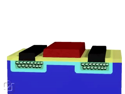
These metal oxide semiconductor field effect transistors are strangely straightfor. # amplification # bjt # diode # doping # n type doping # npn transistor # p type doping # silicon atom # bipolar junction transistor # transistor. It is the time when the drain substrate diode starts to conduct. It is the applied voltages which. We can also observe that, the diffused channel n (between two n+ regions), the insulating dielectric sio 2 and the aluminum metal layer of the gate together form a parallel plate capacitor. This is an improvement over previous versions of. So t 2 will be off with its resistance rsoff = 10^ 10 ohms. When the input is kept low that is at 0 volt, then gate of mosfet t, is at negative potential with respect to the source s 1. The reverse biased pn junction types; Animated diagram showing the operation of a tuned circuit (lc circuit). # amplification # bjt # diode # doping # transistor. Source, own work (original text: Asked by rajasri mundrathi what are the si units of mass, length and time respectively?


.)